Advanced Laser Processing Research Team
Team Director
Koji Sugioka
D.Eng.
Contact
ksugioka [at] riken.jp
Advanced Laser Processing Research Team,
RIKEN Center for Advanced Photonics
2-1 Hirosawa, Wako, Saitama 351-0198 Japan
Related links
Laboratory on RIKEN Website
Advanced Laser Processing Research Team | RIKEN![]()
Outline
Our research team is developing advanced laser processing techniques which realize low environmental load, high quality, high efficiency fabrication of materials. In particular, by using femtosecond lasers, novel material processing techniques including 3D fabrication, surface nanostructuring, novel nanomaterial synthesis, and tailored beam processing are developed, which are applied to fabricate highly functional micro/nanodevices. As one of examples, our team successfully fabricated 3D microfluidic surface enhanced Raman spectroscopy (SERS) chips by combining different types of femtosecond laser processing (hybrid femtosecond laser processing).
The fabricated SERS chips enabled real-time sensing of trace substances as well as ultrasensitive detection of analytes at attomolar-level concentrations. The developed technique will offer high sensitivity diagnosis of diseases such as viral infection and Alzheimer's disease in early stages.
Fields
Engineering, Materials Sciences, Interdisciplinary science and engineering, Multidisciplinary
Keywords
Femtosecond laser, Laser processing, Micro/nanofabrication, 3D fabrication, Biochip
Subjects
- Development of laser-based 3D micro and nanoprocessing and application for fabrication of micro and nanodevices
- Development of high quality, high efficiency, high resolution processing based on beam shaping techniques
- Nanomaterials synthesis and surface nanostructuring by ultrafast lasers
- Elucidation of laser and matter interactions
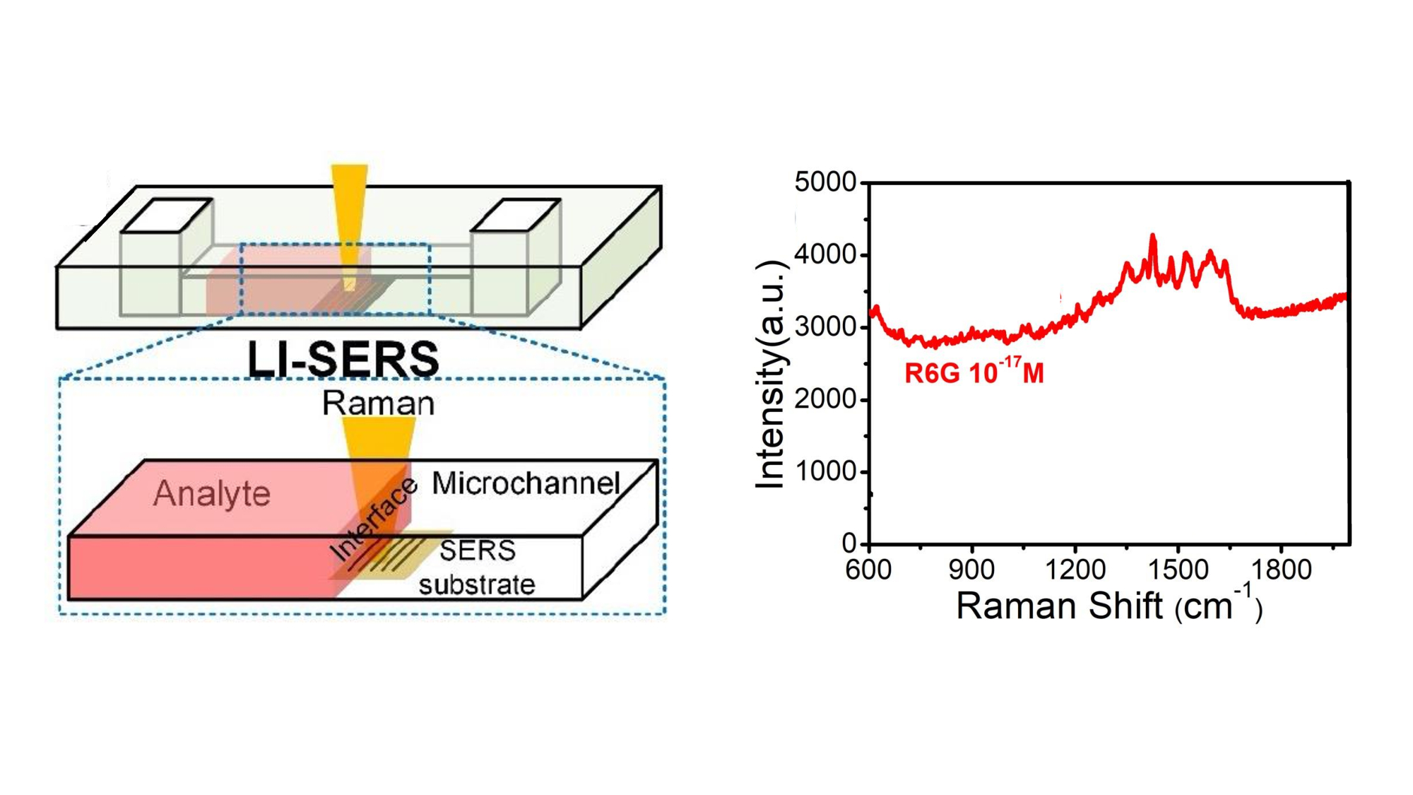
(Left) Schematic illustration of a new SERS sensing scheme (Liquid Interface Assisted SERS: LI-SERS) enabling attomolar sensing. (Right) Analysis of R6G solution at a concentration of 10-17 M by LI-SERS using a microfluidic SERS chip.
Selected Publications
- Zhang, J., Obata, K., Ozasa, K., Uzawa, T., Ito, Y., Sugioka, K.: “Rapid manufacturing of glass-based digital nucleic acid amplification chips by ultrafast Bessel pulses”, Small Sci. 4, 2300166 (2024).
- Kawabata, S., Bai, S., Obata, K., Miyaji, G., and Sugioka, K.: “Two-dimensional laser-induced periodic surface structures formed on crystalline silicon by GHz burst mode femtosecond laser pulses” , Int. J. Extreme Manuf. 5, 015004 (2023).
- Bai, S., Serien, D., Ma, Y., Obata, K., and Sugioka, K.: “Attomolar sensing based on liquid-interface assisted surface enhanced Raman scattering in microfluidic chip by femtosecond laser processing” , ACS Appl. Mater. Interfaces 12, 42328–4233 (2020).
- Bai, S., Serien, D., Hu, A., and Sugioka, K.: “Three-dimensional microfluidic SERS chips fabricated by all-femtosecond-laser-processing for real-time sensing of toxic substances” , Adv. Funct. Mater. 28, 1706262 (2018).
- Wu, D., Xu, J., Niu, L., Wu, S., Midorikawa, K., and Sugioka, K.: “In-channel integration of designable microoptical devices using flat scaffold-supported femtosecond-laser microfabrication for coupling-free optofluidic cell counting” , Light Sci. Appl. 4, e228 (2014).
Publications
Members
| Koji Sugioka | Team Director |
| Kotaro Obata | Researcher |
| Shi Bai | Researcher |
| Jiawei Zhang | Postdoctoral Researcher |
| Ashkan MomeniBidzard | Postdoctoral Researcher |
| Kazunari Ozasa | Special Temporary Research Scientist |
| Shota Kawabata | Junior Research Associate |